Product Summary
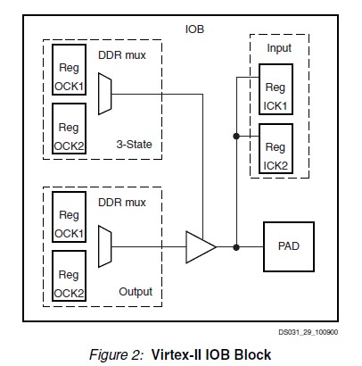
The XC2V30004FF1152I is a member of the Virtex-II family, which is a platform FPGA developed for high performance from low-density to high-density designs that are based on IP cores and customized modules. The XC2V30004FF1152I delivers complete solutions for telecommunication, wireless, networking, video, and DSP applications, including PCI, LVDS, and DDR interfaces. The leading-edge 0.15 μm / 0.12 μm CMOS 8-layer metal process and the XC2V30004FF1152I architecture is optimized for high speed with low power consumption. Combining a wide variety of flexible features and a large range of densities up to 10 million system gates, the Virtex-II family enhances programmable logic design capabilities and is a powerful alternative to mask-programmed gates arrays. The Virtex-II family comprises 11 members, ranging from 40K to 8M system gates.
Parametrics
XC2V30004FF1152I absolute maximum ratings: (1)VCCINT, Internal supply voltage relative to GND: –0.5 to 1.65 V; (2)VCCAUX, Auxiliary supply voltage relative to GND: –0.5 to 4.0 V; (3)VCCO, Output drivers supply voltage relative to GND: –0.5 to 4.0 V; (4)VBATT, Key memory battery backup supply: –0.5 to 4.0 V; (5)VREF Input reference voltage: –0.5 to VCCO + 0.5 V; (6)VIN, Input voltage relative to GND (user and dedicated I/Os): –0.5 to VCCO + 0.5 V; (7)VTS, Voltage applied to 3-state output (user and dedicated I/Os): –0.5 to 4.0 V; (8)TSTG, Storage temperature (ambient): –65 to +150 ℃; (9)TJ, Maximum junction temperature: +125 ℃.
Features
XC2V30004FF1152I features: (1)Industry First Platform FPGA Solution; (2)IP-Immersion Architecture; (3)SelectRAM Memory Hierarchy; (4)High-Performance Interfaces to External Memory; (5)Arithmetic Functions; (6)Flexible Logic Resources; (7)High-Performance Clock Management Circuitry; (8)Active Interconnect Technology; (9)SelectIO Ultra Technology; (10)Supported by Xilinx Foundation and Alliance Series Development Systems; (11)SRAM-Based In-System Configuration; (12)0.15 μm 8-Layer Metal Process with 0.12 μm High-Speed Transistors; (13)1.5V (VCCINT) Core Power Supply, Dedicated 3.3V VCCAUX Auxiliary and VCCO I/O Power Supplies; (14)IEEE 1149.1 Compatible Boundary-Scan Logic Support; (15)Flip-Chip and Wire-Bond Ball Grid Array (BGA); (16)Packages in Three Standard Fine Pitches (0.80 mm,1.00 mm, and 1.27 mm); (17)Wire-Bond BGA Devices Available in Pb-Free Packaging ; (18)100% Factory Tested.
Diagrams

 |
 XC2V1000 |
 Other |
 |
 Data Sheet |
 Negotiable |
|
||||||
 |
 XC2V1000-4BG575I |
 |
 IC FPGA VIRTEX-II 575PBGA |
 Data Sheet |

|
|
||||||
 |
 XC2V1000-4BGG575C |
 |
 IC VIRTEX-II FPGA 1M 575-MBGA |
 Data Sheet |

|
|
||||||
 |
 XC2V1000-4BGG575I |
 |
 IC FPGA VIRTEX-II 2M 575-MBGA |
 Data Sheet |

|
|
||||||
 |
 XC2V1000-4FF896I |
 |
 IC FPGA VIRTEX-II 896FCBGA |
 Data Sheet |

|
|
||||||
 |
 XC2V1000-4FFG896C |
 |
 IC VIRTEX-II FPGA 1M 896-FBGA |
 Data Sheet |

|
|
||||||
 (Hong Kong)


